Why GaN for DC-DC Space Designs
Power electronics engineers are constantly working towards designs with higher efficiency and higher power density while maintaining high reliability and minimizing cost. Advances in design techniques and improved component technologies enable engineers to consistently achieve these goals. Power semiconductors are at the heart of these designs and their improvements are vital to better performance. In this EPC space blog, we will demonstrate how GaN power semiconductors allow for innovation in the harsh radiation environments of space applications.
GaN power semiconductors offer designers in the high reliability market a sudden and significant improvement in electrical performance over their silicon power MOSFET predecessors. Table 1 compares radiation hardened GaN and Si power semiconductor device characteristics important for circuit designers to increase efficiency and power density in their converter.
| 200 V GaN FBG20N18B | 200 V Si MOSFET | Technology Comparison | |
| VDS (V) | 200 | 200 | Same |
| RDS(ON) (mΩ) | 26 | 28 | Similar |
| Device Area (mm2) | 23 | 237 | 10 x Reduction |
| QG (nC) | 6 | 240 | 40 x Reduction |
| QGD (nC) | 2 | 60 | 30 x Reduction |
| QGS (nC) | 2 | 70 | 35 x Reduction |
| COSS (pF) @50 V VDS | 300 | 900 | 3 x Reduction |
| COSS (pF) @1 V VDS | 950 | 10000 | 10 x Reduction |
| QRR (nC) | 0 | 11700 | Infinite Reduction |
| VSD (V) | 1.75 | 1.2 | 1.5 x Increase |
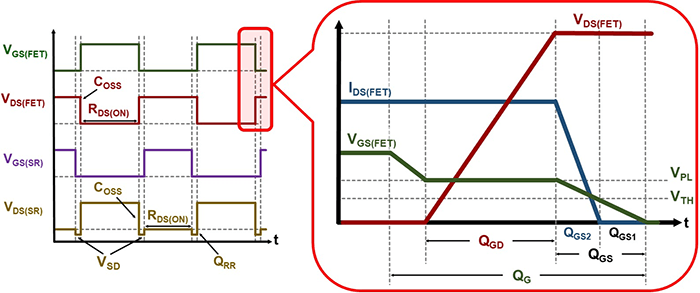
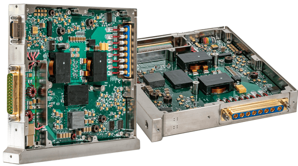
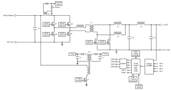
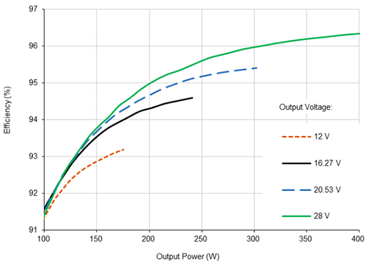
While the comparisons in Table 1 clearly show the benefits of a new power semiconductor technology, it is hard to estimate how this will translate into real world circuit performance where the power semiconductor is part of a larger system. We will explain the theoretical impact of these device characteristics on converter performance using the power semiconductor commutation diagram in Figure 1 and describe the impacts on an innovative real-world product design using the VPT SGRB10028S DC-DC converter, shown in Figure 2. The SGRB10028S has a 100 V input, an adjustable single output from 12 V to 28 V, output power up to 400 W, and efficiencies above 96%. The SGRB Converter employs a Phase-Shifted Full Bridge circuit topology with GaN devices used for both the primary devices and the secondary synchronous rectifiers.

Starting from the first entry in Table 1, VDS, the maximum drain-to-source blocking voltage of the power semiconductor. VDS must be large enough to support the off-state drain-to-source voltage shown in Figure 1 with adequate margin; this also includes circuit voltage ringing, introduced mainly by parasitic inductances in the circuit. Most of the blocking voltage is dependent on the isolation transformer leakage inductance spike and the design input and output voltages. Thus, for GaN and Si designs, the voltage stresses, and therefore maximum drain-to-source blocking voltage will be the same.
RDS(ON), or device on-state drain-to-source resistance, determines conduction losses. In this design example, a high current is required to reach the high-power demands and the lowest on-resistance devices available are selected, which are similar between GaN and Si power semiconductors at 26 mΩ and 28 mΩ, respectively. While the on-resistance is similar, the device area and PCB space required by the power semiconductors are very different. The GaN power semiconductor is about one-tenth of the size of the Si MOSFET. In this design, shown in Figure 2, the GaN power semiconductor occupies roughly 5-10% of the board space on one side of the design; if the designer had to use a 10x larger Si MOSFET, the board space occupied would jump to over 50%. This would greatly impact the design of the other components, in particular the magnetics, forcing them to become smaller and limiting the use of integrated magnetics, both of which increase losses and degrade converter efficiency. Advantages like this do not show up in Table 1 and Figure 1 but have a major impact on system performance.
As device size shrinks, the losses must reduce proportionally to avoid becoming the thermal bottleneck in the design. The remainder of Table 1 relates to switching related losses that occur during a switching cycle. QG, gate charge, is the total amount of charge required to turn on the device, shown in Figure 1. For the GaN device, QG is 40x lower than the Si device, resulting in lower gate drive losses. Another benefit of lower gate drive loss is a reduction in power required by an auxiliary power supply, which often occupies notable board space and has non-negligible power loss. QGD, gate-to-drain charge, often referred to as Miller charge, is the amount of charge during voltage commutation, shown in Figure 1. For the GaN device, QGD is 30x lower than the Si device, resulting in lower voltage commutation losses. QGS, gate-to-source charge, is the amount of charge to reach the device threshold voltage (QGS1) and rise to the Miller plateau voltage (QGS2), shown in Figure 1. For the GaN device, QGS is 35x lower than the Si device, resulting in lower current commutation losses, which occur in the QGS2 timing of Figure 1. COSS, output capacitance, is the sum of drain-to-source and gate-to-drain capacitance. Output capacitance must be discharged or soft-commutated during each switching cycle. For the GaN device, COSS is 3 to 10 x lower than the Si device, respectively for high (50 V) and low (1 V) blocking voltages. In hard switching applications, output capacitance loss is related to VDS2 and the higher blocking voltage output capacitance condition is of more importance. In soft-switching applications, where soft-switching is generally achieved in relation to VDS, the larger output capacitance value, which occurs at lower blocking voltages is of more importance. Regardless of the design topology, the GaN device has lower COSS related losses. QRR, reverse recovery, is the stored charge in the body diode of a MOSFET that must be discharged before the MOSFET can block voltage and is a major source of loss in a synchronous rectifier (SR). For the GaN device, which has no minority carriers and zero QRR, reverse recovery losses are infinitely lower than the Si device. VSD, source-to-drain forward voltage, also known as body diode forward voltage in MOSFETs, is the conduction voltage when a synchronous rectifier device is off and must conduct current, generally a short dead time before the control device is commanded on as shown in Figure 1. For the GaN device, the forward conduction losses are 1.5x higher than a Si device. Detailed weighting of each of these loss mechanisms is application dependent and beyond the scope of this blog, but regardless of the application GaN has significantly lower charges/capacitances and associated losses compared to a Si MOSFET. For the design shown in Figure 2, the GaN power semiconductor losses are reduced by a large enough factor that, at only 1/10th the size of a Si MOSFET, the GaN device is still not the thermal bottleneck of the system. This achievement is not possible without a superior power semiconductor.


Combining advanced GaN power semiconductors and state of the art design techniques enables a new level of performance in high reliability space designs as demonstrated in Figure 2. The VPT SGRB series have been designed specifically for space-borne telecommunications where high efficiency, low noise, and radiation tolerance are imperative. Using advanced GaN-based technology, the SGRB series was developed to provide a solution that increases power supply efficiency, resulting in reduced system size, weight, and cost. This GaN-based SGRB series of DC-DC converters earned the Military & Aerospace Electronics Innovators Awards Platinum recognition, its highest honor. This distinction recognizes companies in the aerospace and defense electronics industries that have made groundbreaking contributions and innovative solutions to solve design challenges.


