Webinar Recap – GaN in Space

A few weeks ago, Efficient Power Conversion hosted a webinar titled GaN in Space. Following the presentations there were very lively Q&A sessions with EPC’s CEO and co-founder, Alex Lidow. Below are the most frequently asked questions from the two sessions and the corresponding responses.
Q: What is the recommended derating for space applications?
A: Everybody has their own philosophy about derating. EPC tests all devices to 100% and they are tested to failure to make sure that there is adequate margin above the datasheet limit. EPC’s Phase 11 reliability report has more details on test to failure. By testing parts to the point of failure an understanding of the amount of margin between the data sheet limits can be developed, and more importantly, an understanding of the intrinsic failure mechanisms can be found. By knowing the intrinsic failure mechanisms, the root cause of failure, and the device’s behavior over time, temperature, electrical or mechanical stress, the safe operating life of a product can be determined over a more general set of operating conditions.
Q: What testing is performed to certify GaN devices and to what spec’s?
A: EPC SPACE performs 100% screening on all space level parts according to an equivalent MIL-PRF-19500 with some modification pertaining to eGaN technology and flip-chip packaging including sample accelerated mechanical and electrical tests.
Q: Do EPC Space products have any space heritage?
A: Yes, both EPC and EPC Space products have space heritage. EPC SPACE devices are currently being used and designed into low earth orbit (LEO), geosynchronous equatorial orbit (GEO), and deep-space exploratory missions. For additional information on this, please contact [email protected]
Q: How do customers deal with EMI caused by the very fast switching of GaN?
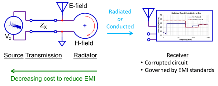
A: There is a video on the EPC website (How to GaN 014) that extensively covers this topic. It explains the three reasons that eGaN devices are extremely quiet in EMI.
One of the reasons is they have very low inductance. If you buy a chip scale part, they have no inductance since there is no package. Therefore, you get very low voltage overshoot when you switch the devices on and off. It is the overshoot that generates a lot of EMI. The EMI is proportional to the current and the voltage in the ringing overshoot. If you cut the overshoot in half or to one third you will cut your EMI generation by a quarter or a ninth.
The second reason is that GaN devices have no diode recovered charge (QRR = 0). The recovered charge in a hard switching circuit using a MOSFET means that the diode takes a while for it to recover. While it’s doing that it’s generating a huge amount of EMI. More actually than the voltage overshoot in most circuits. GaN doesn’t have this loss.
The third source of EMI is the energy generated by the fast rise and fall times. In the video there are two examples of 5 ns rise and fall and 1 ns rise and fall and if you have zero overshoot and no QRR a 1ns rise and fall time puts the noise generated out over 1 GHz which is pretty easy to filter out. If you are at 5 ns then it’s out at 200 MHz, still easy to filter out.
In summary, you don’t generate EMI because you don’t have a lot of voltage overshoot because of package inductance, you don’t generate it because you don’t have the diode recovery, and high switching speed is a way to push the EMI out to very high frequencies where it is very easy to filter. Despite their significantly faster switching speeds, eGaN FETs generate less EMI than MOSFETs.
Q: How do customers handle dv/dt or di/dt in critical applications like these space applications?
A: One thing about GaN is that the dv/dt’s and di/dt’s are faster than ever before. These devices have dv/dt’s like 300 V/ns and di/dt’s like 200 A/ns and even more than that which raises a lot of questions. EPC has a primary application that exploits this; Lidar applications desire the highest current in the shortest pulse widths and eGaN devices can generate 100 A+ pulses that are 2ns wide. That equates to about 0.5 ns rise and 0.5 ns fall time across an 80 V BUS. These are very high di/dt and dv/dt and EPC wanted to determine if any new failure mechanisms would be created by this. To answer that question, EPC developed a test system that uses multiple racks of devices that are being pulsed under maximum conditions. The methodology and results are detailed in the Phase 11 reliability report. To date, the parts have been taken out to 12 trillion cycles with no failures. EPC will continue testing them out to the point where they start to fail so that a failure mechanism can be identified.
Q: Can you talk about integration in GaN and the current test plan for the high side gate drivers that were recently announced?
A: EPC has several integrated GaN products. Some of them are custom devices for specific customers and others you can buy commercially. EPC recently introduced the commercial EPC2152, which includes monolithic half bridge with drivers, control logic, and boot strap circuit. These are rated for input voltages of 80 V, 15 A output current with a heatsink and have run up to 3 MHz. The devices are very fast, very efficient, and very small. The EPC2152 has been gamma tested well above 10 Megarads with no deterioration. They haven’t yet been single event tested because it will take a design change to achieve single event immunity. EPC Space is beginning to work on a RadHard version design. Please contact EPC Space for more information if this is of interest to you.