
What is up with the SS (Source Sense) Pin?

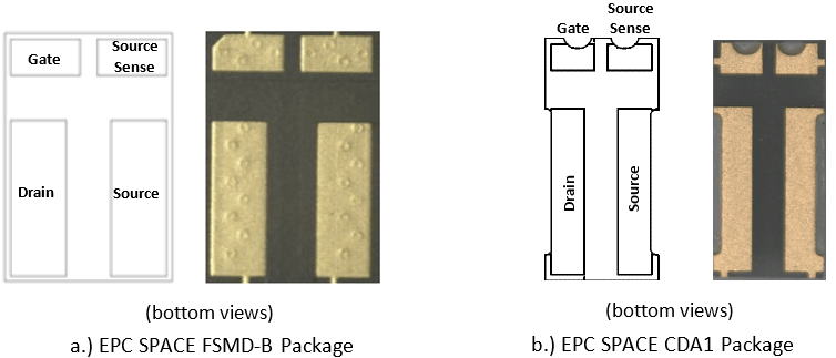
A quick look at any discrete eGaN® high electron mobility transistor (HEMT) shows that each package contains a SS (Source Sense) pin. This post is an explanation as to why that vitally important pin is necessary and provided to help extract the maximum switching and efficiency performance from the EPC Space HEMTs. As an example, the position of the SS pin on the FSMD-B and CDA1 packages is shown in Figure 1.
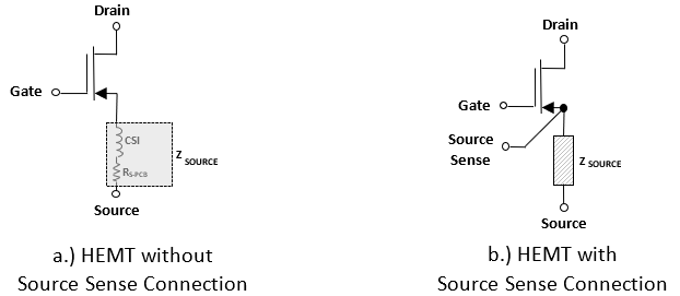
The Source Sense pad is connected directly to the source on the die internal to the package – a true Kelvin connection, thus eliminating unwanted drain (load) current and gate (drive) current interactions. Internal to the package, the Source and Source Sense pads have the same reference potential, that of the Source of the internal eGaN HEMT transistor. The gate drive loop is thus independent from any interactions caused by the packaging impedance, Zsource (the package and PCB DC resistance and common-source inductance (CSI)) when there is no SS connection provided. Figure 2 illustrates the connection of the Source Sense pin within the HEMT packaging.
Why is the Source Sense Pin Needed?
When there is no Source Sense connection, the gate driver circuitry must be referenced to the Source pin. This causes a “two loop” interaction between the high-frequency gate drive current and drain current signals, algebraically summed as the source current. The gate-source drive voltage signal fights the voltage across Zsource, transiently reducing the amount of gate drive voltage available to the HEMT. This gate and drain current interaction results in reduced operating efficiency, or erratic turn-on and turn-off operation in the worst case.
Adding the Source Sense pin creates a connection directly to the Source connection of the internally packaged die. The impedance Zsource is virtually eliminated. The voltage drive signal presented to the gate-source of the HEMT is as “pure” as possible. It is impacted ONLY by the inductance created by the loop area of the gate, the external gate resistance (if any is used), the internal gate resistance of the HEMT, the impedance of the gate driver to ground, or to the 5V drive potential and the input capacitance (Ciss) of the HEMT. This is an R-L-C circuit that may be damped with the external gate resistance selected. By using the Source Sense, the characteristics and waveshape of this voltage loop is now controlled (damped) by the circuit designer.
When using the Source Sense pin the gate-source drive signal has far less under-shoot and over-shoot during switching transients than the case where no SS pin is available. The gate of the HEMT experiences far less transient-related voltage stress and excellent gate drive fidelity – thus operating efficiency and reliability is improved. This simple, single pin affords the circuit designer the means to extract every bit of performance that the EPC Space discrete products have to offer. As you can plainly see, having the SS pin available just makes perfect “sense”!

