Mitigation of Ionizing Radiation Degradation in Linear Regulators Using eGaN HEMTs
by Diego de Azcuénaga
An analysis of structural immunity to Total Ionizing Dose (TID) and control loop stability in high-reliability linear regulation architectures.
Traditional space LDOs rely on silicon MOSFETs that suffer from radiation degradation. To solve this, Tony Marini from EPC Space highlights a revolutionary alternative using enhancement-mode Gallium Nitride (eGaN) HEMTs. Their unique material physics inherently resists Total Ionizing Dose (TID) effects without performance loss, ensuring exceptional parameter stability in harsh orbital environments.
GaN Physics and Radiation Mitigation Mechanisms
Unlike silicon MOSFETs, which rely on physical oxide interfaces that trap positive charges when exposed to low-dose ionizing radiation (<30 kRad), eGaN HEMTs feature a wide bandgap structure devoid of such vulnerable gate oxides. In silicon devices, this trapped charge reduces the transconductance (gm) by 20% or more, forcing the analog voltage control loop to constantly adjust over wide operating margins to maintain regulation.
In contrast, Tony Marini emphasizes that eGaN HEMTs are virtually immune to low-dose radiation. The transconductance—defined in Siemens as the ratio of change in drain current to the change in gate-source voltage (ΔId /ΔVgs)—exhibits a typical decrease of less than 3% under equivalent low-dose exposure. Because gm closely follows the gate-source threshold voltage (Vgs(th)) performance, this physical resilience prevents the regulator’s analog control loop from “hunting” across a broad voltage range to achieve stable output regulation.
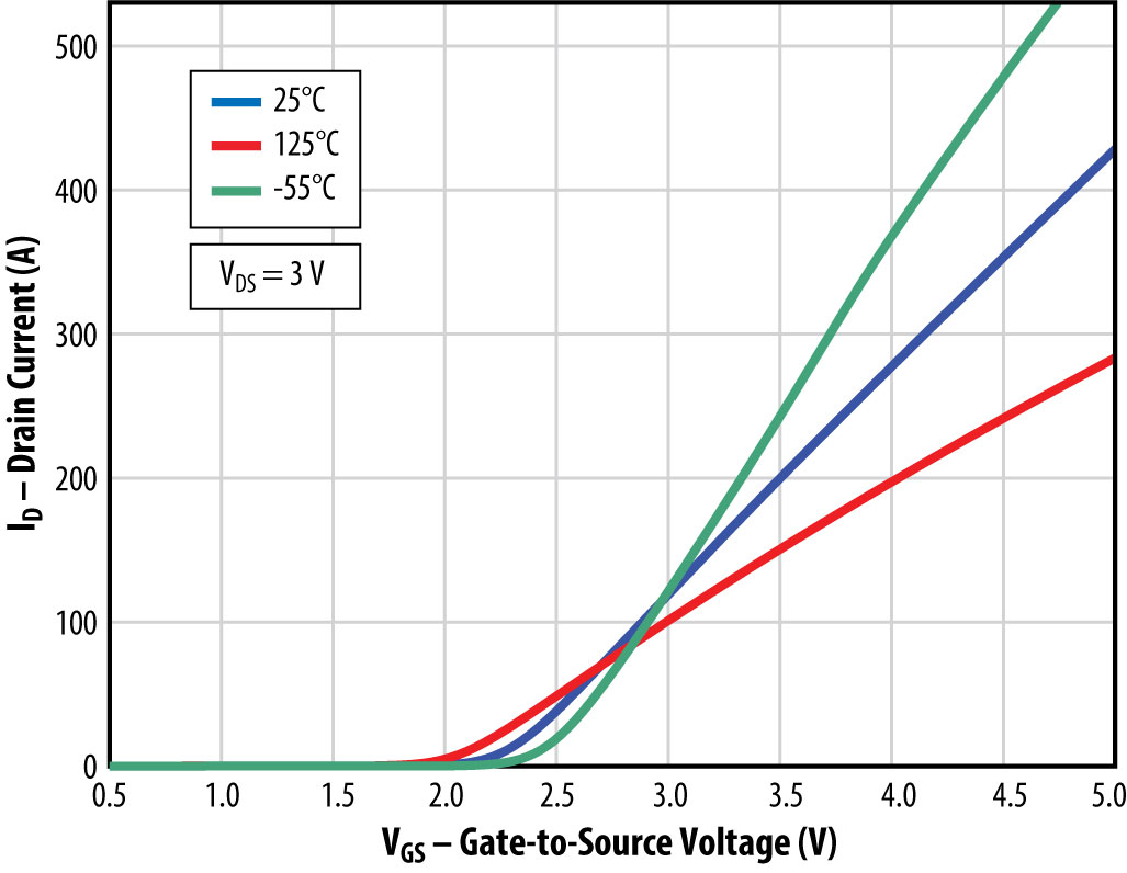
The typical transfer characteristics (Figure 1) that define the stability of these systems are anchored in the specific behavior of the pass elements under distinct temperatures and biasing configurations, as detailed in the technical data provided by EPC Space.
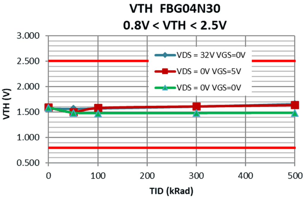
Furthermore, experimental evaluation demonstrates that the threshold voltage (Vth) remains remarkably flat across extensive Total Ionizing Dose (TID) testing profiles. Figure 2 illustrates the robust operational envelope of a representative eGaN HEMT device (such as the FBG04N30 platform) under continuous exposure up to 500 kRad.
Gate Biasing Challenges and Structural Implementation
Because eGaN HEMTs are exclusively available as n-channel polarity devices, implementing them as pass elements introduces specific biasing constraints. To maintain proper linear regulation, the bias potential provided to the gate terminal must remain slightly higher than the combined magnitude of the output voltage and the maximum gate-source voltage required at full load current:
Vbias > Vout + Vgs (Id(max))
According to the insights shared by Marini, the exceptional stability of Vgs against aging, temperature swings, and radiation allows designers to set the required gate bias potential as low as possible. For instance, in a system configured for a regulated 5.0 Vdc output, a stable gate bias potential of approximately 8.5 V (relative to the circuit’s ground return) can be safely utilized. This tight tolerance window minimizes overhead power consumption and safeguards the error amplifier stage from unnecessary voltage stresses.
Evaluation Boards Architecture & Interface
Implementing eGaN HEMTs as pass elements in linear regulation architectures requires a detailed analysis of their circuit environment and control interfaces. EPC Space designed two evaluation platforms, designated as the EPC7C023 (optimized for an operating regime up to 5 A) and the EPC7C024 (designed for an operating regime up to 0.5 A). The purpose of these boards is to serve as test vehicles to isolate and study the physical behavior of GaN devices operating within the linear region.
Control Loop Topology and Semiconductor Selection
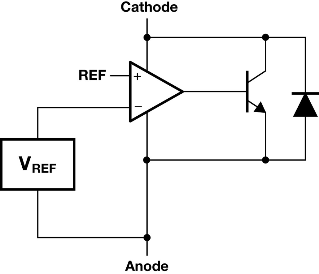
To prevent complex compensation networks from introducing additional variables into the semiconductor’s analysis, a fundamental analog control loop was implemented based on the TL1431 integrated circuit. This component operates as a shunt regulator that integrates both the error amplifier and an internal bandgap voltage reference onto a single silicon die, whose internal topology is detailed in the block diagram of Figure 3.
The differentiation in current conduction capacity between the two platforms relies exclusively on the sizing of the eGaN HEMT used as the power pass element (Qpass):
- High-Current Platform (EPC7C023): Integrates the EPC7019G device, characterized by a maximum voltage rating of 40 V, a current capacity of 90 A, and a fully-enhanced drain-source on-resistance (Rds(on)) of 4.5 mΩ.
- Low-Current Platform (EPC7C024): Employs the EPC7014UB device, dimensioned for lower-magnitude analog precision loads.
Tony Marini emphasizes that the pass transistor never operates in a fully-enhanced state during active regulation. If the HEMT turned on completely, it would act as a closed switch and lose its ability to modulate drain current via gate-source voltage, causing the control loop to lose regulation. Therefore, the nominal Rds(on) of 4.5 mΩ serves only as an asymptotic limit to approximate resistance at the saturation boundary and estimate the minimum dropout voltage.
Analytical Modeling of Dropout Voltage and Parasitic Variables
The theoretical minimum dropout voltage (Vdo(min)) of this architecture is determined by summing the ohmic losses across the partially enhanced semiconductor channel and the voltage drop across the series-connected current sense resistor (Rcs):
Vdo(min) ≅ Iout . (Rds(on_sat) + Rcs)
Applying the specific parameters of the EPC7C023 board under a maximum load of 5 A yields the following initial calculation:
- Approximate drop across the HEMT (EPC7019G): ≅22.5 mV.
- Drop across the sense resistor (Rcs = 10 mΩ): 50 mV.
- Theoretical lower dropout limit: 72.5 mV.
Physical characterization of the circuit on the test bench revealed an actual measured dropout voltage of 152 mV, representing a deviation from the simplified mathematical model. Marini explains that this increase stems from real-world physical factors in thermal and geometric modeling: primarily the distributed parasitic resistance within the PCB copper traces (PCB copper etch resistance) and the fact that the EPC7019G HEMT enters hard saturation at a slightly lower Vgs potential than theoretically estimated under static linear biasing conditions.
Layout Thermodynamics and Parasitic Suppression on the PCB
To manage continuous linear power dissipation (PD = (Vin – Vout) . Iout) without bulky heatsinks, the PCB utilizes planar Vishay ThermaWick aluminum nitride (AlN) components (designated as TH1–TH4 in Figure 4). Four elements are populated on the 5 A board (EPC7C023) for lateral heat routing, while none are required on the 0.5 A variant (EPC7C024).
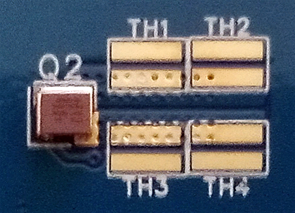
Regarding signal integrity and stability against high-frequency transients, the presence of parasitic inductances and capacitances poses a risk of oscillation at the control (gate) node. The implemented physical countermeasure consists of minimizing current loop areas by routing the power lines connected to the drain and source of the pass element with copper traces that are as short and wide as possible, reducing both DC resistance and electromagnetic noise coupling.
Monitoring Interface Configuration and Transfer Equation
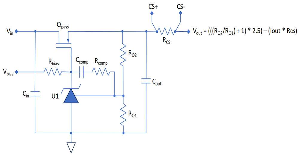
Each board exposes six power terminals (Vin±, Vout±, VBIAS±) and high-impedance differential pads (CS+/CS-). To isolate the native GaN dropout, the sense resistor (Rcs = 10 mΩ for EPC7C023; 50 mΩ for EPC7C024) sits outside the feedback loop. No dedicated enable pin exists; dropping Vbias to 0 V serves as the turn-off mechanism.
The electrical coupling of all these variables is consolidated in the circuit schematic analyzed in Figure 5. The regulated output voltage (Vout) follows:
Vout = ((Ro2/Ro1) + 1) . 2.5 V – (Iout . Rcs)
Performance Verification & Test Results
Control Loop Simulation and Stability Analysis
Prior to finalizing the bill of materials (BOM) for the evaluation boards, Tony Marini notes that the control loop’s voltage regulation performance was verified via LTSPICE numerical simulation. To validate stability without early overhead, the implementation utilized a standard, historical simulation model of the TL1431 IC controller acting as the analog error amplifier and bandgap reference.
Instead of validating loop margins via standard frequency-domain Bode plots, Marini utilized the time-domain load transient response to prove system stability. The loop compensation architecture, using a simple parallel resistor-capacitor network, was kept as unadorned as possible. This minimalist baseline prevented external compensation parameters from masking the raw, intrinsic performance of the eGaN HEMT pass transistor.
Load Transient Response Verification
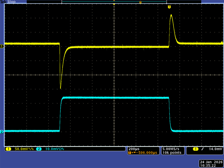
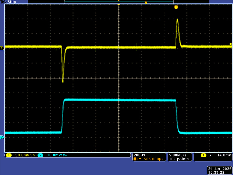
The physical transient verification proved that both platforms exhibit fast recovery windows and remain entirely free of control loop oscillations across their maximum step-change boundaries.
| Metric | EPC7C023 (5 A Version) | EPC7C024 (0.5 A Version) |
| Output Current Step Range | 100 mA to 5 A | 10 mA to 500 mA |
| Peak Voltage Deviation Amplitude | ~160 mV | ~110 mV |
| Response / Recovery Time | ~50 µs | ~40 µs |
High-Current Subsystem (EPC7C023) Performance
For the large-die HEMT configuration (EPC7019G), the load current was stepped across virtually its full operating range, spanning from 0.1 A to 5 A. As captured in the hardware test data below (Figure 6), the control loop dampens the step transition within ~50 µs, maintaining a tight peak voltage deviation of only ~160 mV.
Low-Current Subsystem (EPC7C024) Performance
For the smaller-die HEMT variant, the transient load step was verified from 0.05 A to 0.5 A. Driven by a tighter internal parasitic capacitance profile, the voltage loop recovers within ~40 µs, restricting the maximum voltage deviation to a nominal 110 mV (Figure 7).
Value Proposition & Broadband System-Level Implications
The demonstrated performance of eGaN HEMTs in continuous linear regulation alters high-reliability aerospace design trade-offs. Traditionally, spacecraft power distribution networks require separate semiconductor qualification pipelines for high-frequency payloads and continuous DC regulation. Proving that eGaN technology can operate as a stable, radiation-tolerant LDO pass element enables broad architectural consolidation beyond localized efficiency parameters.
Spectral Versatility: Unifying DC and RF Power Infrastructure
The core architectural benefit highlighted by Tony Marini revolves around the broadband utility of the GaN substrate. While Gallium Nitride has established a definitive role in high-frequency switching power converters and RF power amplifiers, its deployment in zero-frequency (DC) analog applications completes a crucial design continuum.
This spectral versatility yields significant advantages for spaceflight systems:
- Component Qualification Consolidation: Utilizing a single, inherently radiation-hardened semiconductor technology across the DC-to-RF frequency spectrum reduces the overhead associated with establishing diverse component qualification lifecycles.
- Elimination of Radiation Shielding Mass: The structural immunity to Total Ionizing Dose (TID) degradation simplifies structural design. Designers can omit heavy localized spot shielding around linear voltage regulators feeding sensitive payloads.
- System Drift Redundancy Mitigation: Because the physical control nodes do not undergo the radiation-induced charge-trapping typical of silicon-oxide interfaces, the need for complex digital calibration or telemetry compensation networks to correct for rail drift over long mission lifespans is eliminated.
Minimization of Worst-Case Design Margins
Silicon linear regulators require over-designed loops to counter orbital parameter drift. Conversely, the eGaN control loop maintains stable, oscillation-free transient responses without complex compensation because its transconductance thresholds remain unchanged over the spacecraft’s operating life. This proves eGaN HEMTs act as reliable continuous DC regulation elements, giving aerospace designers a single, uniform semiconductor platform handling everything from direct current to microwave frequencies.
Implementation Guidelines
The verification of eGaN HEMTs within LDO linear regulator topologies provides a clear framework for high-reliability aerospace power distribution networks. By evaluating the structural boundaries, thermal dynamics, and loop behavior analyzed in the preceding sections, designers can implement unified guidelines to maximize system reliability in hostile orbital environments.
Component Implementation Guidelines
To replicate the deterministic, oscillation-free performance recorded on the evaluation hardware, space-grade system layout execution must adhere to three strict design constraints:
- Gate Drive Impedance and Stray Inductance Control: Due to the high transconductance (gm) of eGaN devices, any parasitic inductance at the gate terminal can couple with the internal capacitances to induce high-frequency ringing. Gate routing traces must be minimized to short, wide geometries, and placed on the same PCB layer as the analog error amplifier whenever possible.
- Dynamic Thermal Layout Decoupling: Linear pass elements operating under constant input-to-output voltage differentials face continuous thermal dissipation (PD = ΔV . Iout). Designers must maximize the use of planar ceramic helper pads (such as aluminum nitride structures) to route heat laterally into internal board copper planes, preventing localized hot spots from shifting the operating thresholds of surrounding low-voltage reference circuits.
- External Sense Resistor Placement: To preserve the native, uncompensated dropout voltage performance of the GaN substrate, the current sense resistor must remain physically outside the closed voltage feedback loop. However, designers must account for its continuous series ohmic loss when calculating the total worst-case dropout ceiling at the system level.
Conclusions
Integrating eGaN HEMTs into linear regulation architectures successfully bridges a critical gap in spacecraft power infrastructure. This architecture demonstrates that Gallium Nitride is no longer restricted to high-frequency switching converters or RF payloads; it can operate as a reliable, stable pass element for continuous DC regulation.
Ultimately, this structural validation allows aerospace engineers to implement a single, unified semiconductor platform across the entire DC-to-RF frequency spectrum. Consolidating the component procurement lifecycle, eliminating local radiation shielding mass, and removing end-of-life parameter drift margins allow for the development of lighter, more efficient, and highly ruggedized power electronics optimized for deep-space and long-duration orbital missions.